Indexed In
- Open J Gate
- Genamics JournalSeek
- Academic Keys
- JournalTOCs
- ResearchBible
- China National Knowledge Infrastructure (CNKI)
- Scimago
- Ulrich's Periodicals Directory
- Electronic Journals Library
- RefSeek
- Hamdard University
- EBSCO A-Z
- OCLC- WorldCat
- SWB online catalog
- Virtual Library of Biology (vifabio)
- Publons
- MIAR
- Scientific Indexing Services (SIS)
- Euro Pub
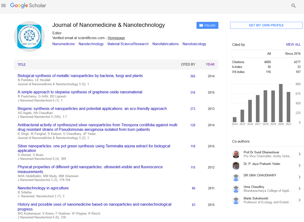
- Google Scholar
Useful Links
Share This Page
Journal Flyer

Open Access Journals
- Agri and Aquaculture
- Biochemistry
- Bioinformatics & Systems Biology
- Business & Management
- Chemistry
- Clinical Sciences
- Engineering
- Food & Nutrition
- General Science
- Genetics & Molecular Biology
- Immunology & Microbiology
- Medical Sciences
- Neuroscience & Psychology
- Nursing & Health Care
- Pharmaceutical Sciences
Nano-analysis of transition metal/silicon interface
3rd International Conference on Nanotek & Expo
December 02-04, 2013 Hampton Inn Tropicana, Las Vegas, NV, USA
Mohammed Ibrahim, P. Stender, Z. Balogh and G. Schmitz
Accepted Abstracts: J Nanomed Nanotechnol
Abstract:
Atom probe tomography (APT) is a microscopic technique which has a unique capability to analyze thin films reactions in 3D. It has an outstanding resolution of 0.05 nm in depth and 0.01 nm laterally. In addition to that, the chemical/isotopic nature of the species is determined with the aid of time of flight (TOF) mass spectrometry. The technique works on the principle of field evaporation from a sample in the shape of sharp needle. Lateral distribution of the evaporated atoms is gained by position sensitive detector. The depth profiling is calculated from the data sequence and the shrinkage of the sample during field evaporation. The standard APT with high voltage pulses was limited to the highly conductive metals and alloy, but with the introduction of short laser pulses, APT overcomes the limitations and now the analysis semiconductors, insulating materials and even polymers became possible. In this work, the interfaces atomic structure between transition metals (M) and amorphous Silicon (a-Si) at M/a-Si/M sequence have been investigated using Laser-assisted atom probe tomography (APT). An intermixed zone was measured with a more or less continuous transition and around 6?1 nm width is observed for the M on a-Si stacking. In contrast, a much sharper interface of less than 1.4?0.4 nm width for the a-Si on top of M. This asymmetric behavior was found to be even more pronounced after a short (10-30 min) annealing at temperatures higher than the deposition temperature (room temperature). The same behavior was observed in case of planer geometry investigated by SNMS, which confirms the existence of the asymmetric behavior.
Biography :
Mohammed Ibrahim completed his M.Sc. at the age of 26 years from Linkoping University-Sweden in 2006. He is now a Ph.D. student at University of Muenster-Germany.


