
Indexed In
- Open J Gate
- JournalTOCs
- RefSeek
- Hamdard University
- EBSCO A-Z
- OCLC- WorldCat
- Scholarsteer
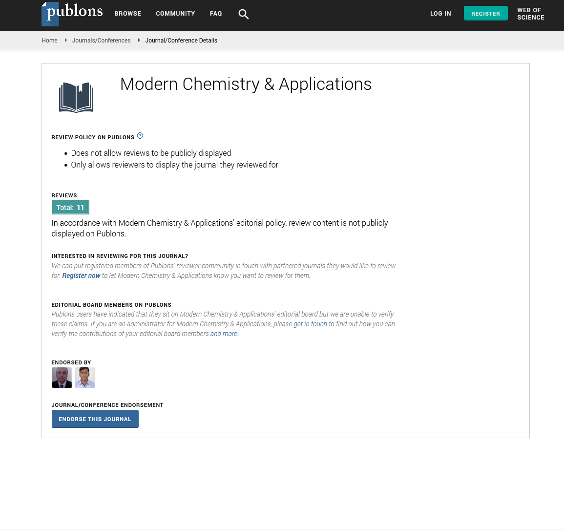
- Publons
- Geneva Foundation for Medical Education and Research
- Google Scholar
Useful Links
Share This Page
Journal Flyer
Open Access Journals
- Agri and Aquaculture
- Biochemistry
- Bioinformatics & Systems Biology
- Business & Management
- Chemistry
- Clinical Sciences
- Engineering
- Food & Nutrition
- General Science
- Genetics & Molecular Biology
- Immunology & Microbiology
- Medical Sciences
- Neuroscience & Psychology
- Nursing & Health Care
- Pharmaceutical Sciences
Commentry - (2023) Volume 11, Issue 3
Low-Temperature Bonding for Stress Mitigation in Silicon and Gallium Arsenide Integration
Baxendell Kagan*Received: 24-May-2023, Manuscript No. MCA-23-21793; Editor assigned: 26-May-2023, Pre QC No. MCA-23-21793 (PQ); Reviewed: 12-Jun-2023, QC No. MCA-23-21793; Revised: 20-Jun-2023, Manuscript No. MCA-23-21793 (R); Published: 28-Jun-2023, DOI: 10.35248/2329-6798.23.11.420
Description
Low-temperature bonding has emerged as a significant technique in the field of silicon and gallium arsenide integration, offering a promising solution for stress mitigation in semiconductor devices. The integration of silicon and gallium arsenide materials has gained significant attention due to their unique properties and potential applications in various electronic and optoelectronic devices.
Thermal analysis of Si/GaAs bonding wafers
The thermal analysis of Si/GaAs bonding wafers aims to understand the temperature-induced stress and strain that occurs during the bonding process. Silicon and gallium arsenide have different Coefficients of Thermal Expansion (CTE), with Si having a higher value compared to GaAs. When subjected to temperature variations, the resulting thermal mismatch between the two materials generates stress at the interface.
The initial bonding stress arises during the cool-down phase after the bonding process. The stress is mainly caused by the difference in the CTEs of Si and GaAs and can result in deformations and structural defects in the wafers. This stress is particularly critical when bonding large area wafers or bonding multiple layers of materials.
Mitigation strategies for bonding stresses
To mitigate the bonding stresses and enhance the reliability of Si/GaAs bonded wafers, several strategies can be employed,
Thinning of the Si wafer: One effective approach is to reduce the thickness of the Si wafer before bonding. Thinning the Si wafer decreases its thermal expansion mismatch with GaAs, reducing the overall stress generated during temperature variations. However, caution must be exercised to avoid excessive thinning that can compromise the mechanical integrity of the wafer.
Low-temperature bonding: Performing the bonding process at a lower temperature can help alleviate bonding stresses. By reducing the temperature, the thermal expansion mismatch is minimized, leading to lower stress at the interface. This approach requires precise control over the bonding process parameters and the selection of appropriate bonding materials.
Intermediate bonding layers: Introducing an intermediate bonding layer between Si and GaAs can serve as a stress buffer. Materials such as polyimide or Benzocyclobutene (BCB) with a matched CTE to Si and GaAs can act as compliant layers, absorbing the stress generated during temperature changes. The choice of the intermediate layer material should consider compatibility, process integration, and electrical/optical properties.
Redistribution of stresses: Another approach is to redistribute the stresses by incorporating patterned structures or trenches on the bonding surface. These patterns can act as stress relief mechanisms, allowing stress concentration at specific regions rather than spreading throughout the wafer. Careful design and optimization of pattern geometries are essential to ensure effective stress redistribution.
Post-bonding annealing: Performing a post-bonding annealing process can help relax the residual stresses in the bonded wafer. Annealing at an appropriate temperature for a specific duration allows the bonded interface to adjust and relieve the stress, thereby improving the mechanical stability of the wafer.
The thermal analysis of Si/GaAs bonding wafers reveals the challenges associated with the thermal expansion mismatch between the two materials, leading to significant bonding stresses. To address these challenges, various mitigation strategies have been developed, including wafer thinning, low-temperature bonding, intermediate bonding layers, stress redistribution techniques, and post-bonding annealing. The combination of these strategies can enhance the reliability of Si/GaAs bonding stresses are a significant concern in the integration of Si and GaAs wafers, the implementation of appropriate mitigation strategies is significant to ensure successful bonding and reliable device performance. By considering the thermal expansion mismatch and utilizing techniques such as wafer thinning, low-temperature bonding, intermediate bonding layers, stress redistribution, and post-bonding annealing, manufacturers can minimize the impact of bonding stresses and improve the overall quality of Si/GaAs bonded wafers.
Citation: Kagan B (2023) Low-Temperature Bonding for Stress Mitigation in Si/GaAs Integration. Modern Chem Appl. 11:420.
Copyright: © 2023 Kagan B. This is an open-access article distributed under the terms of the Creative Commons Attribution License, which permits unrestricted use, distribution, and reproduction in any medium, provided the original author and source are credited.