Indexed In
- Open J Gate
- JournalTOCs
- RefSeek
- Hamdard University
- EBSCO A-Z
- OCLC- WorldCat
- Scholarsteer
- Publons
- Geneva Foundation for Medical Education and Research
- Google Scholar
Useful Links
Share This Page
Journal Flyer

Open Access Journals
- Agri and Aquaculture
- Biochemistry
- Bioinformatics & Systems Biology
- Business & Management
- Chemistry
- Clinical Sciences
- Engineering
- Food & Nutrition
- General Science
- Genetics & Molecular Biology
- Immunology & Microbiology
- Medical Sciences
- Neuroscience & Psychology
- Nursing & Health Care
- Pharmaceutical Sciences
Short Communication - (2023) Volume 11, Issue 3
COP-Free Effect of a Dislocation-Free Ingot Grown by the NOC Method
Kazuo Nakajima1*, Masami Nakanishi2, Martin Su2 and Chuck Hsu22GlobalWafers Co Ltd. No.8, Industry E. Rd. II, Hsinchu Science Park, Hsinchu 30075, Taiwan
Received: 05-May-2023, Manuscript No. MCA-23-21196; Editor assigned: 08-May-2023, Pre QC No. MCA-23-21196 (PQ); Reviewed: 22-May-2023, QC No. MCA-23-21196; Revised: 29-May-2023, Manuscript No. MCA-23-21196 (R); Published: 06-Jun-2023, DOI: 10.35248/2329-6798.23.11.413.
Introduction
The NOC (Noncontact Crucible) method has been proposed to grow Si single ingot with a large diameter ratio (diameter of ingot/ diameter of crucible=0.9) without contact with a crucible wall [1]. In this method, a large and deep low-temperature region was effectively established in a Si melt using an insulator plate set under the bottom of the crucible [2]. In the field of Si fine semiconductor, a COP (Crystal Originated Particle) free Si ingot is quite important because COPs become obstacles for the fine exposure technology of ultrafine semiconductor devices (2nm width). We found that the position of cross point between concentration curves of vacancy and interstitial Si atom is a key factor and quite effective for NOC growth to largely reduce void (crystal defect formed by agglomeration of vacancies) or COP (pits caused by micro-void with the SC-1 cleaning) in a Si ingot [3]. This may provide another way in the field.
Growth of Defect-Free Ingot by CZ (CZOCHRALSKI) Method
Figure 1 shows the concentration of vacancy, CV and interstitial Si atom, CI (Z) near critical point as a function of growth rate, V. The temperature gradient, G is used as a parameter. To reduce COP completely to 0, V/G or V must be controlled very precisely within quite narrow region closed to the critical point. Pv and Pi are regions with quite low vacancy and interstitial Si atom, respectively. The defect-free crystal is made up of the Pv and Pi regions. This is the commonly used method which requires precise controllability.
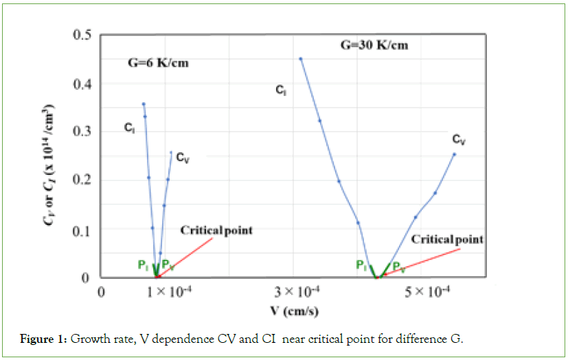
Figure 1: Growth rate, V dependence CV and CI near critical point for difference G.
Growth of Defect-Free Ingot by NOC Method
The NOC method has the temperature gradient with two stages, G1at the growing interface and G2 at the melt surface. Figure 2 shows the schematic illustration of temperature gradients, CV and CI (Z) in NOC and Cz ingots as a function of the distance from the growing interface. The temperature gradie nt in the NOC ingot has a relatively gradual slope compared with that in the Cz ingot which grows above the melt surface [3]. The position of cross point between the CV and CI (Z) curves is quite important for NOC growth. The position for NOC growth is lower than that for Cz growth. To largely reduce COP in a Si ingot, the cross point should be lowered to the limit. The NOC method has a potential to largely lower the temperature of cross point. As the result, the residual defect concentration can be fundamentally approximated to zero. This is the simple mechanism to reduce COP to the limit in a NOC ingot.
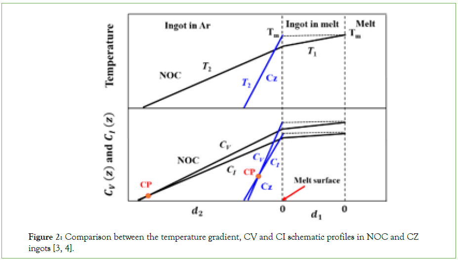
Figure 2: Comparison between the temperature gradient, CV and CI schematic profiles in NOC and CZ ingots [3,4].
An ingot was grown by the NOC method as shown in Figure 3 [4]. The length and diameter ratio are 15cm and 0.66, respectively. On the top part of ingot, 4 (111) facet planes were observed. Liner habit lines appeared through the body to tail parts, which were clear evidence for dislocation-free.
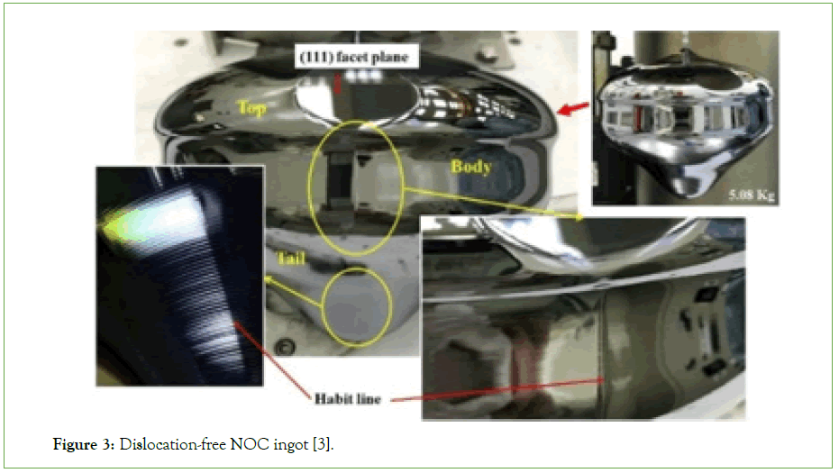
Figure 3: Dislocation-free NOC ingot [3].
For confirmation, no EPDs (Etch-Pit Density of Dislocations) were also observed at all over the ingot. The point-defects have possibility to be largely reduced by selecting proper ratio between the temperature gradients at the melt surface and at the growing interface using the NOC method [4]. For this ingot, from its cooling curve, most of vacancies can be regraded to be changed to voids in most parts of the ingot. The distribution of Bulk Micro Defect (BMD) oxygen precipitate (SiO~2) with stress in crystal, Bulk Stacking Fault (BSF) stacking fault caused by stress of excessive oxygen precipitate (SiO~2)) and Oxidation Induced Stacking Fault (OISF) stacking fault on (111) face caused by larger stress in the cross section of the dislocation- free NOC ingot is shown in Figure 4. Many small white points and many a little bit long rod-shaped white points can be observed as BMD and BSF, respectively. The boundaries between BMD and BSF can be known by precise observation. A ring-OISF can be observed in the BSF region and is distributed along the periphery of ingot. The H band which contains BMD and BSF can be observed inside the ring- OISF, which is not shown in Figure 4.
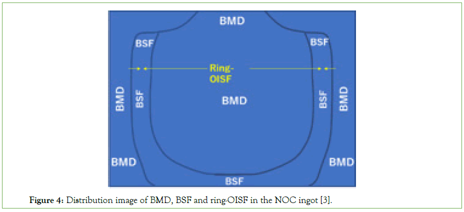
Figure 4: Distribution image of BMD, BSF and ring-OISF in the NOC ingot [3].
For the evaluation of COP, a B-doped (4.8 m Ω cm) NOC single wafer with 6φ inch was used. The distribution of COP was evaluated by the particle counter (counting size: 0.12 μm) together with the SC (Standard Clean)-1 cleaning whose process was repeated 5 times. This cleaning process can little bit etch the surface of the wafer. Figure 5 (a) shows the trend of counting number (Figure 5).
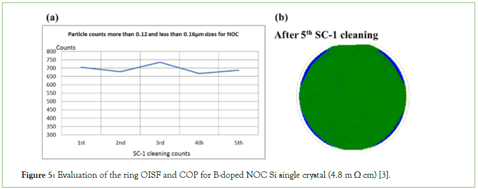
Figure 5: Evaluation of the ring OISF and COP for B-doped NOC Si single crystal (4.8 m Ω cm) [3].
The particle count more than 0.12 μm and less than 0.16 μm which corresponds to COP almost keeps constant after every cleaning. This means that COPs were not revealed from the inside wafer by the etching effect of the SC-1 cleaning because COPs did not exist inside wafer. Figure 5 (b) shows the distribution of particles obtained by the particle counter for the same wafer after 5th etching. No particles larger than 0.12 μm appeared all over the wafer. This also means COPs do not exist in this wafer. Quite few I-defects were also observed in the NOC ingot [3].
Merits and Demerits of the NOC Method
Comparing to the Cz method, to get COP-free ingot, this method requires the more simple mechanism and no precise control of V or G because lowering the cross point is only main factor to obtain such an ingot and it is more simple compared to keeping the critical point. Enough lowing the cross point can attain the complete and uniformly reduction of vacancy and interstitial Si atom. Only demerit of this method is the present furnace provides relatively lower growth rate.
Conclusion
The new mechanism to reduce COP to its limit was proposed without precise control near critical point. It was proved by the growth of dislocation-free NOC ingot and the characterization about COP distribution over the ingot. The mechanism contains the position control of cross point which should be lowered to the limit. The ingot grown on this mechanism does not have COPs and have quite few I-defects. The present method may provide a way to obtain a Si ingot with uniformly and minimally distributed point defects. The grow rate is limited by the expanding rate of low- temperature region. To largely increase the growth rate for practical use, how to maintain stability of the expanding rate is important.
References
- Nakajima K, Ono S, Kaneko Y, Murai R, Shirasawa K, Fukuda T et al. Applications of novel effects derived from Si ingot growth inside Si melt without contact with crucible wall using noncontact crucible method to high-efficiency solar cells. J Cryst Growth. 2017;468:705-709.
- Nakajima K, Ono S, Itoh H. Concept and method to create a distinct low-temperature region in a Si melt for growth of a Si single ingot with a large diameter ratio using the noncontact crucible method. J Cryst Growth. 2018;499:55-61.
- Nakajima K, Nakanishi M, Su M, Hsu C. Two-dimensional BMD, BSF, ring-OISF and COP distributions in a dislocation-free ingot grown by the NOC method. J Cryst Growth. 2023;605:127064.
- Nakajima K, Nakanishi M, Su M, Hsu C. Two-dimensional distribution of vacancy concentration at cross points for the ingot length and the temperature gradients to largely reduce point defects and the growth of a dislocation-free NOC ingot for evaluation of its quality. J Cryst Growth. 2022;592:126721.
Citation: Nakajima K, Nakanishi M, Su M, Hsu C (2023) COP-Free Effect of a Dislocation-Free Ingot Grown by the NOC Method. Modern Chem App. 11:413.
Copyright: ©2023 Nakajima K, et al. This is an open-access article distributed under the terms of the Creative Commons Attribution License, which permits unrestricted use, distribution, and reproduction in any medium, provided the original author and source are credited.
