Indexed In
- Open J Gate
- Genamics JournalSeek
- Academic Keys
- JournalTOCs
- ResearchBible
- China National Knowledge Infrastructure (CNKI)
- Scimago
- Ulrich's Periodicals Directory
- Electronic Journals Library
- RefSeek
- Hamdard University
- EBSCO A-Z
- OCLC- WorldCat
- SWB online catalog
- Virtual Library of Biology (vifabio)
- Publons
- MIAR
- Scientific Indexing Services (SIS)
- Euro Pub
- Google Scholar
Useful Links
Share This Page
Journal Flyer

Open Access Journals
- Agri and Aquaculture
- Biochemistry
- Bioinformatics & Systems Biology
- Business & Management
- Chemistry
- Clinical Sciences
- Engineering
- Food & Nutrition
- General Science
- Genetics & Molecular Biology
- Immunology & Microbiology
- Medical Sciences
- Neuroscience & Psychology
- Nursing & Health Care
- Pharmaceutical Sciences
Research Article - (2024) Volume 15, Issue 1
CHARACTERIZATION OF Au(111) AND HOPG SUBSTRATES BY SPM
Antonio Canseco Urbieta*, Gabriel Sanchez Gruz, Ivonne Arisbeth Diaz Santiago, Fernando Mejia Zarate, Francisco Emanuel Velasquez Hernandez, and Yosemik Arjuna Leon NataretReceived: 02-Jan-2024, Manuscript No. jnmnt-23-24023; Editor assigned: 05-Jan-2024, Pre QC No. jnmnt-23-24023(PQ); Reviewed: 17-Jan-2024, QC No. jnmnt-23-24023(QC); Revised: 25-Jan-2024, Manuscript No. jnmnt-23-24023(R); Published: 30-Jan-2024, DOI: 10.35248/2157-7439.24.15.706.
Abstract
One of the tools for topographic characterization is Scanning Probe Microscopy (SPM). For the morphological studies of gold substrates with face 111 [Au (111)] and Highly Ordered Pyrolytic Graphite (HOPG) Atomic Force Microscopy (AFM) and Tunneling Effect Microscopy (STM) were used. As a result of the visualization and characterization of the Au (111) substrate we have: gold grains with measurements of 359 nm from AFM and gold terraces with heights of 0.2 nm by STM. In the HOPG substrate we observed by AFM terraces with measurements of 0.359 nm and by STM carbon atoms with interatomic distances of 0.2727 nm.
Keywords
Au; HOPG; Substrates; AFM and STM
INTRODUCTION
There is a wide variety of substrates suitable to be visualized with AFM and STM. Among the main criteria taken into account for their study are the possible contamination problems that may occur during the experimental work, that their properties are homogeneous over the entire surface and that they are free of possible defects, that they are flat and no more than five micrometers in roughness [1].
Material growth studies usually consist of the controlled deposition of a given number of atoms or molecules on a well-characterized crystalline substrate, usually single crystal or highly oriented surface. Some frequently used substrates are graphite, silver, platinum, and gold in the form of solid crystals or thin films.
The description of the growth mechanisms at the atomic scale has been largely based on the Terraces-Step-Klink (TSK) model (Figure 1). In this figure, a step indicated with a red line is shown, which separates the upper or lower terraces in the image, and shows a corner site (kink) in the middle of it. On the other hand, the same Figure 1 shows several fundamental entities of the film growth such as an atom (ad-atom) and a dimer (ad-dimer) adsorbed on the surface of the upper or lower terraces, respectively. In addition, a vacancy and a four-atom island can be observed on such terraces [1,2].
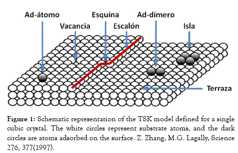
Figure 1: Schematic representation of the TSK model defined for a single cubic crystal. The white circles represent substrate atoms, and the dark circles are atoms adsorbed on the surface. Z. Zhang, M.G. Lagally, Science 276, 377(1997).
Au (111) substrate
The gold surface represents an excellent substrate because it does not oxidize easily and remains clean for long periods of time. For this reason, gold is considered the most noble metal, not very reactive with atoms or molecules, which at the gas/liquid interface have a fcc (face-centered cubic cell 111) crystal structure.
Gold is an attractive substrate for surface science studies due to its chemical inertness, it has also become an increasingly important material in industrial applications due to its unique combination of properties; for example, its corrosion resistance, which makes it the ideal metal for electrical contacts and its potential applications in heterogeneous catalysis. The availability of high-quality oriented substrate surface is a key element in the preparation of nanostructures with tunable properties. One can approach this task with the highest precision and through self-organization on patterned substrates. The Au (111) surface is constituted by the accumulation of gold atoms that form grains. These have an approximate dimension of 3. 238 μm, however, the last layers of the upper part are formed by steps or long terraces with surface (111).
The herringbone reconstruction of Au (111), is a classic example of a substrate surface that offers well-ordered matrix adsorption sites [3-7].
The hydrophilic character of the clean Au (111) surface [4] is supported by the experimental work of Haywar and Trapnel, carried out in 1964; where it was shown that the elements of the periodic table have different reactivities with gases, except gold, which has no reactivity with hydrogen, oxygen and nitrogen. On the other hand, it does have reactivity with carbon monoxide, methanol and water [5].
The affinity of this metal for water gives it a hydrophilic character on its surface, especially on the (111) [6] side. This character is related to the surface tension, since the higher the surface tension, the more hydrophilic the material is. In the case of gold, the surface tension is 1410 ergs/cm2, and 72.75 ergs/cm2 in water [7]. The efficient test to determine the hydrophilic or hydrophobic character of materials is based on the contact angle between the liquid (water) and the metal surface. For hydrophilic surfaces, the contact angle should be between 0-90 degrees. A higher degree corresponds to hydrophobic materials (Figure 2) [8].
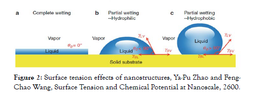
Figure 2: Surface tension effects of nanostructures, Ya-Pu Zhao and Feng- Chao Wang, Surface Tension and Chemical Potential at Nanoscale, 2600.
Highly ordered pyrolytic graphite (HOPG)
Highly ordered pyrolytic graphite (HOPG) is a two-dimensional solid, with strong covalent bonding in the basal planes of the carbon and weak Van der Waals interaction between the layers. HOPG is ideal for molecular imaging studies because it is a conductive substrate, weakly interacting, high purity (which provides microscopists with an atomically smooth surface), is characterized by sp2, the two is exponent type bonds in which the C-C bond length is approximately 0.142 nm and each layer separated by 0.335 nm (Figure 3), in the basal plane have saturated all carbon bonds and is extremely inert with a small energy barrier for adatom diffusion [9-12].
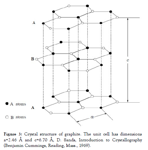
Figure 3: Crystal structure of graphite. The unit cell has dimensions a=2.46 Å and c=6.70 Å, D. Sands, Introduction to Crystallography (Benjamin Cummings, Reading, Mass., 1969).
The HOPG surface forms very useful substrates for the growth of metal nanoparticles due to the inert nature of this surface (Figura-3). HOPG is selected as a substrate for the study of adsorption of molecules on surfaces because of its relatively weak interaction with the adsorbate and its easy cleavage results in large flat terraces. It has long been shown that organic molecules with long alkyl chains can be immobilized on the basal plane of HOPG [13-15].
HOPG is an ideal test for STM since atomic resolution is possible even in air conditions. The first controversy, the triangular symmetry observed in STM versus the known hexagonal HOPG structure, was resolved early on by taking into account that STM images are measurements of the electron density near the Fermi energy and not of the actual surface topography. Thus, the ABAB, HOPG stacking produces atomic symmetry breaking in two different types of atoms. The α atoms, with a reduced electron density around the Fermi level due to the presence of a direct neighbor in the subsurface layer, and the β atoms, which suffer the opposite effect due to the lack of such a neighbor. Under these conditions, STM images show predominantly only β atoms, giving rise to the actually observed HOPG structure characterized by a triangular symmetry [16-19].
The HOPG can be considered as the drosophila of surface science, especially for scanning probe studies. It is composed of stacked twodimensional hexagonal Bernal lattices with carbon atoms popularly known as graphene layers. Due to the weak Van der Waals bonding between the HOPG layer, the top layer can be displaced or rotated by mechanical or chemical means. It is commonly accepted that, as a result of the rotation of the top layer, superperiodic structures are called moiré patterns for HOPG surfaces [20,21].
METHODOLOGY
Specialized equipment such as; AFM innova bruker S/N 1B38A, STM innova bruker S/N 1B38A, stereo microscope, Milli-Q Millipore, as well as different specialized glassware materials were used in the procedures.
Au(111) substrate
On Au (111) substrate, 1.4 cm x 1.1 cm Au substrates with a thickness of 150 nm with (111) face were used, which consist of a concentrated gold film on mica plate which consists of a 100% polycrystalline thin layer of gold atoms in the preferential (111) direction (Figure 4).
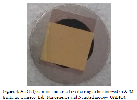
Figure 4: Au (111) substrate mounted on the ring to be observed in AFM (Antonio Canseco, Lab. Nanoscience and Nanotechnology, UABJO).
The substrate does not need to be cleaned or polished, and its preparation consists of heating to dark red in a butane flame for 5 minutes and cooling to room temperature. During this process the surface takes on a morphology characterized by flat monocrystalline zones (terraces).
HOPG substrate
Graphite is black to the naked eye and has a layered structure (Figure 5). Each graphene layer is composed of a planar arrangement of carbon atoms, forming a honeycomb [22].
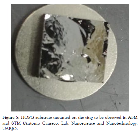
Figure 5: HOPG substrate mounted on the ring to be observed in AFM and STM (Antonio Canseco, Lab. Nanoscience and Nanotechnology, UABJO.
RESULTS AND DISCUSSION
Visualization of single-crystalline solid substrates
Au (111) substrate: To characterize the morphology of the Au (111) substrate, in the experimental part the scan that was worked was 10 micrometers with the AFM (Figure 6), where defined gold grains and grains in the form of islands can be seen, with a measurement of 359 nm.
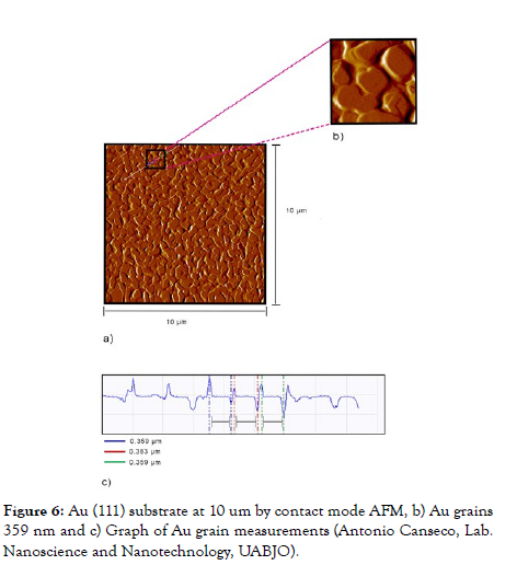
Figure 6: Au (111) substrate at 10 um by contact mode AFM, b) Au grains 359 nm and c) Graph of Au grain measurements (Antonio Canseco, Lab. Nanoscience and Nanotechnology, UABJO).
The observed terraces of the Au substrate (111) was 0.2 nm (Figure 7) by STM, which corresponds to the height of the Au atom.
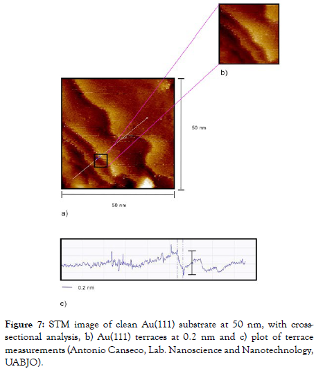
Figure 7: STM image of clean Au(111) substrate at 50 nm, with crosssectional analysis, b) Au(111) terraces at 0.2 nm and c) plot of terrace measurements (Antonio Canseco, Lab. Nanoscience and Nanotechnology, UABJO).
HOPG substrate
The HOPG sample presents terraces in which a step is observed crossing the image diagonally; these terraces are ideal for deposition studies given their area. With the cross-sectional analysis, the height was calculated to be 1.7 nm (Figure 8, item a). The side bar of the image is interpreted as follows: the lighter area corresponds to the upper part of the image and the dark area corresponds to the lower part of the image, this principle is for all the images presented in this research (Figure 8, item b).
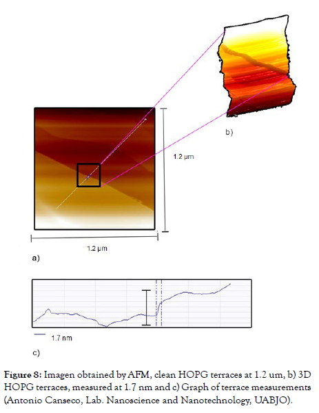
Figure 8: Imagen obtained by AFM, clean HOPG terraces at 1.2 um, b) 3D HOPG terraces, measured at 1.7 nm and c) Graph of terrace measurements (Antonio Canseco, Lab. Nanoscience and Nanotechnology, UABJO).
Figure 9 shows an atomic resolution image of the HOPG, in which the triangular and/or hexagonal structures, normally observed in STM images of graphite, are observed. The HOPG is excellent for the calibration of interatomic distances, and thanks to it we can calculate the horizontal distances of any atom or molecule under study.
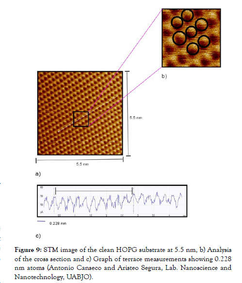
Figure 9: STM image of the clean HOPG substrate at 5.5 nm, b) Analysis of the cross section and c) Graph of terrace measurements showing 0.228 nm atoms (Antonio Canseco and Aristeo Segura, Lab. Nanoscience and Nanotechnology, UABJO).
Analysis of Au (111) and HOPG substrates
The measurements of the gold grains (Figure 6) observed from the AFM in contact mode were 359 nm, these results are congruent with those found in the literature, specifically coinciding with the studies developed by Zhi Hui Liu since in them they found grains larger than 250 nm [23,24].
The characteristic description of the growth mechanism at atomic scale is based on the terrace-step-corner model, [1,2] this pattern was observed in the Au (111) substrate by STM with a measurement of 0.2 nm (Figure 7) which represents the height of the gold atom.
Likewise, morphological studies of the HOPG were carried out using the same microscopes; as a first point, the terraces were observed by contact mode AFM, of which we can highlight that they are separated by layers of the same substrate and have a theoretical measurement of 0.335 nm reported by the researcher R. C. Tatar.21 In our experiment we reported measurements of 0.333 nm (Figure 8), which coincides with the studies developed by R. C. Tatar. In a second point, (Figure-9) shows a representative image of the HOPG atoms by STM. In the same, the hexagonal arrangement and the distance of the β-type atoms with measurements of 0.2727 nm can be appreciated. It is important to note that in the hexagonal structure the presence of an atom can be observed in the center, since it represents the layer below the first layer. This type of image and information has been previously recorded by various researchers, among others, by Moreno López [9,15]. Comparative analysis of Au (111) and HOPG substrates (Table 1).
| Substrate | Microscope | Cleaning | Form | Literature parameter | Experimental measurement |
|---|---|---|---|---|---|
| Au (111) | AFM | N/A | Grain | 60 a 1800 nm23,24 | 359 nm |
| Au (111) | STM | N/A | Atoms | 0.238 nm1,2 | 0.2 nm |
| HOPG | AFM | Layer removal | Laminate | 0.335 nm21 | .333 nm |
| HOPG | STM | Layer removal | Atoms | 0.284 nm9,15 | 0.2727 nm |
(Table- 1) Comparison of theoretical and experimental measurements of Au (111) and HOPG substrates
CONCLUSIONS
The morphological studies observed on the single crystalline surfaces of Au (111) and HOPG substrates by Scanning Probe Microscopy were as follows:
With AFM, gold grains of the Au (111) substrate were observed, which presented measurements of 359 nm. And with the STM gold terraces were observed presenting measurements of 0.2 nm, corresponding to the height of a gold atom.
In the HOPG terraces were observed by AFM, which presented measurements of 0.335 nm, corresponding to a monolayer of carbon atoms. Also by STM interatomic measurements of 0.272 nm were observed. It is worth mentioning that, from this experiment, triangular and/or hexagonal patterns were identified, which are characteristic of HOPG.
It should be noted that atomic resolution was obtained inS both substrates.
Acknowledgments
The authors thank the Faculty of Chemical Sciences of the Benito Juárez Autonomous University of Oaxaca for the facilities provided for the start of this nanotechnology project.
REFERENCES
- Zhang Z, Lagally M G. Atomistic processes in the early stages of Thin-Film growth. Science.1997; 276(5311): 377-383.
- Passegi, M C G. Estudio de materiales nanoestructurados mediante microscopia de efecto túnel.2011
- Hammer B, Nørskov J K. Why gold is the noblest of all the metals. Nature. 1997; 376(6537):238-240.
- Xiong Xiaoron, Hanein Yael, Weihua Wang, Electrical Engineering Deparment, Chemical Engineering Department University of Washington. Seattle. (44)98195-2500.
- Masel Richard I. Principles of adsorption and reaction on solid Surface. Jhon Wiley and Sons. (1996) 113-12.
- Masel Richard I. White M L. The wetting of gold surfaces by water1. The Journal of Physical Chemistry.1964; 68(10): 3083-3085.
- Somorjai Gabor A. Introduction to Surface chemistry and catalysis. Jhon Wiley and Sons.1993; (47) 273-274.
- Balss Karma M, Avedisian C Thomas, Cavicchi Richard E, Langmuir. 21 (2005):10459-10467.
- López, J C M, Passeggi, M C G, Ferrón J. Surface superstructures in highly oriented pyrolytic graphite surfaces after AR+ bombardment. Surface Science.2008; 602(3): 671-676.
- Zhang J, Hu, Q, Huang W. The observation and new mechanism of an anomalous superperiod on a HOPG surface. Applied Physics A.1998; 66(S1):1129-1131.
- Ying-Jie Zhu, Terra A, Hansen J , Phys Chem. B 2001; 105: 7632-7638.
- Wang Z, Zeng Q, Luan Y, Wu X, Wan L, Wang C G L, et al. Voltage-Dependent scanning tunneling microscopy images of a copper complex on graphite. Journal of Physical Chemistry B.2003; 107(48): 13384-13388.
- Ignacio Lopez-Salido, Dong Chan Lim J. Phys Chem. B 2006; 110(53): 1128-1136.
- López, J C M. FORMACIÓN DE SUPERESTRUCTURAS POR BOMBARDEO IÓNICO EN GRAFITO TIPO HOPG. ResearchGate.2007
- Suzuki Y, Enoki H, Akiba E. Observation of HOPG by STM and contact AFM in various gas atmospheres under pressures up to 1.1MPa. Ultramicroscopy.2005; 104(3-4): 226-232.
- M Hugentober, S Bonnani, Eur Phys J. 2011; 215-220.
- Yıldız, D, Gürlü O. Apparent corrugation variations on moiré patterns on highly oriented pyrolytic graphite. Materials Today Communications. 2016; 8, 72-78.
- Stevens F, Kolodny, L A, Beebe T P. Kinetics of Graphite Oxidation: Monolayer and multilayer etch pits in HOPG studied by STM. Journal of Physical Chemistry B.1998; 102(52):10799-10804.
- Patrick DL, Cee V J, Purcell T J, Beebe T P. Defect pinning in monolayer films by highly controlled graphite defects: molecule corrals. Langmuir.1996; 12(7): 1830-1835.
- A Bryant. Imaging in real time with the tunneling microscope.1986.
- R C Tatar ,S Rabii, Tatar, R C Rabii S. Electronic Properties of Graphite: A Unified Theoretical study. Physical review. 1982;25(6):4126-4141.
- Liang H, Cheng F, Sun W, Shao X, Wang. Two-dimensional molecular porous networks constructed by surface assembling. Coordination Chemistry Reviews.2009; 253(23-24): 2959-2979.
- Liu Z H, Brown N M D. Studies using AFM and STM of the correlated effects of the deposition parameters on the topography of gold on mica. Thin Solid Films.1997; 300(1-2): 84-94.
- Liu Z H, Brown N MD. Scanning tunnelling microscopy characterization of gold film surfaces processed using an argon radio frequency (RF) plasma. Thin Solid Films. 1999; 349(1-2): 78-83.
Indexed at, Google Scholar, Crossref
Indexed at, Google Scholar, Crossref
Indexed at, Google Scholar, Crossref
Indexed at, Google Scholar, Crossref
Indexed at, Google Scholar, Crossref
Indexed at, Google Scholar, Crossref
Indexed at, Google Scholar, Crossref
Indexed at, Google Scholar, Crossref
Indexed at, Google Scholar, Crossref
Indexed at, Google Scholar, Crossref
Indexed at, Google Scholar, Crossref
Indexed at, Google Scholar, Crossref
Citation: Urbieta AC, Gruz GS, Santiago IAD, Zarate FM, Hernandez FEV, et al. (2024) Mechanical Properties of NdPrFeB Based Magnetoactive Bisphenol-Free Boron-Silicate Polymers. J Nanomed Nanotech. 15: 706.
Copyright: ©2024 Urbieta AC, et al. This is an open-access article distributed under the terms of the Creative Commons Attribution License, which permits unrestricted use, distribution, and reproduction in any medium, provided the original author and source are credited.
